Support Board
In an OpenPET Support Crate, the custom Support Board is mounted as a backplane on a standard 12-slot VME chassis that accommodates 6U boards. This Support Board primarily plays two roles, depending on the firmware (Fig. 1). In a Detector Unit for a standard- or large-sized system, the Support Board is loaded with detection firmware and acts as a Detector Unit Controller (DUC). In a Coincidence Unit for a standard- or large-sized system, the Support Board is loaded with coincidence firmware and acts as a Coincidence Unit Controller (CUC).
The Support Board also plays a third role for the special case of a small system when it is configured as a Coincidence Detector Unit Controller (CDUC), which interfaces with the detector boards and performs coincidence functions. Basically the CDUC performs the functions of both the CUC and DUC.
Support Board with Detection Firmware
In a Detector Unit, the main purpose of the Support Board with detection firmware (i.e., DUC) is to accept singles event words from multiple Detector Boards, multiplex them, and pass these singles event words to the Coincidence Interface Board. In addition, it provides the control and power for the Detector Boards.
Shown schematically in Fig. 52, the Support Board acting as a DUC services up to 8 Detector Boards. The standard OpenPET Bus IO circuit, as described in Bus IO, connects the Support Board to each Detector Board. Three FPGAs on the Support Board multiplex the singles event words and pass them through the slot 8 Bus IO block to the Coincidence Interface Board. The event multiplexing and forwarding is shared among the three FPGAs (one Main FPGA and two slave IO FPGAs) due to limited pin count. Several other blocks, such as a clock-conditioning block that ensures the fidelity of the system clock, logic analyzer connectors, two RS-232 ports, and diagnostic LEDs, are not shown in Fig. 52.
High-level commands are sent via USB (or alternatively, through Ethernet or Fiber-Optic) from the Host PC to the Coincidence Unit and ultimately down to the Detector Unit Controller’s Main FPGA, which interprets and executes these commands. This execution may involve controlling the Detector Board, such as by loading a program into the FPGA on the DB. Or it may involve higher-level functions, such as performing a calibration by instructing the DB to produce calibration data, analyzing the forthcoming calibration events, computing calibration parameters, and loading these parameters into the detector memory on the DB.
IO FPGAs
There are two slave IO FPGAs on the Support Board. These act primarily as a multiplexer for singles events, each taking up to 16 individual singles events that it can receive in a single time frame and passing up to 4 of them to the Main FPGA. Obviously, there is some possibility for data loss, and the multiplexing algorithm is designed to ensure that this loss is unbiased. Each IO FPGA also serves as a fan-in and fan-out for communication between the Main FPGA and the individual Detector Boards, and the two IO FPGAs can communicate with each other.
The digital signals between each IO FPGA and the Main FPGA are identical to the standard OpenPET Bus IO signals (Fig. 46): lines for the clock and Time Slice Boundary (both directions), 4 control lines, 4 FPGA programming lines, 16 event data lines, and eight user-definable data lines. There are also 32 user-definable digital lines between the two IO FPGAs, 16 sending data in each direction.
Main FPGA
A single physical Main FPGA performs the logical functions of both the master FPGA and the support microprocessor. Its FPGA-like functions are mostly limited to passing events from the IO FPGAs to the Coincidence Interface Board (providing multiplexing, if necessary).
Some of the logic blocks in the Main FPGA can be programmed using Nios II to be identical to microprocessor hardware, which then runs executable files programmed in C. This support microprocessor receives high-level commands from the Host PC via USB (or Gigabit Ethernet or Fiber-Optics), and then interprets and executes these commands. It is responsible for loading all the programs into the IO FPGAs and DB FPGA, as well as the contents of all the support memory, detector memory, and all other registers that are on the DB and SB. It also monitors the event stream and can insert diagnostic information (such as event rates) into the event stream or provide this information directly to the Host PC. Whenever possible, calibration routines are also performed on the support microprocessor.
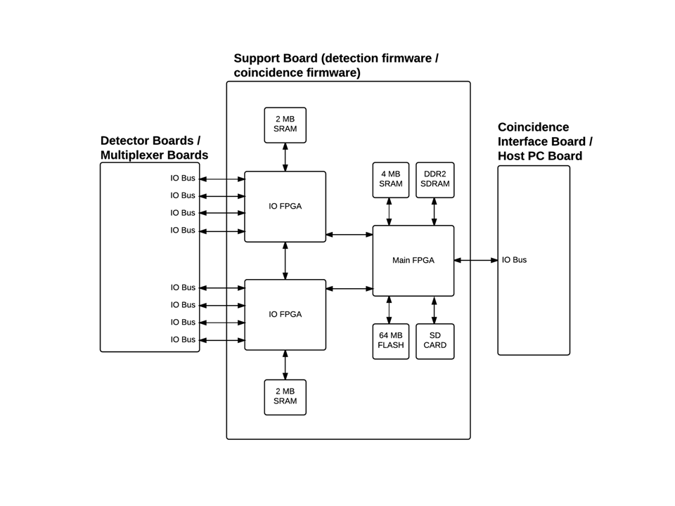
Fig. 52 Schematic of the Support Board, which is loaded with either detection firmware (when used in a Detector Unit) or coincidence firmware (when used in a Coincident Unit.)
Support Memory
There are multiple forms of memory on the Support Board, as shown Fig. 52. The SRAM is accessed by the FPGA and provides its output within 1 clock cycle of being addressed so is both reasonably fast and deterministic, which greatly simplifies incorporating it within FPGA algorithms. However, the SRAM capacity is fairly small. Thus, the Main FPGA is connected to 4 MB of SRAM and each of the IO FPGAs is connected to 2 MB of SRAM, for a total of 8 MB of SRAM on each Support Board. This memory is typically used to store look-up tables that apply real time calibration and corrections to the event data.
As the Main FPGA also emulates a microprocessor, RAM memory and disk storage are also necessary for it to function effectively. The RAM memory is provided via up to 1 GB of RAM that can be plugged into a DDR2 SDRAM connector (identical to that typically found in laptop computers). The disk storage is provided by a SD card (identical to that found in digital cameras) that is plugged into a SD card slot, when users desire disk storage that can be easily removed. Otherwise, standard disk storage is provided by a 64 MB FLASH memory chip that is connected to the Main FPG, in order to store the FPGA firmware needed for DB FPGAs, contents of all the support SRAM memory, detector memory, and all other registers that are on the DB and SB. This information can also be stored in the on-board EPCS memory, which is where it resides in the initial release.
Clock Conditioning
The clock-conditioning block consists of a PLL (phase-locked loop) that regenerates the system clock signal from the Support Board in a Coincidence Unit and passes it to the Support Board FPGAs in a Detector Unit and then to the Detector Boards. The block also includes space for a local clock oscillator, which is used to provide the system clock when the system is being used without a Coincidence Unit (i.e., when the support microprocessor passes events directly to the Host PC).
Connectors
The clock-conditioning block consists of a PLL (phase-locked loop) that regenerates the system clock signal from the Support Board in a Coincidence Unit and passes it to the Support Board FPGAs in a Detector Unit and then to the Detector Boards. The block also includes space for a local clock oscillator, which is used to provide the system clock when the system is being used without a Coincidence Unit (i.e., when the support microprocessor passes events directly to the Host PC).
Slots 0-7
Slots 0-7 in a Detector Unit each contain a Detector Board. Details on the function and design of the Detector Board are available in Detector Board.
Slots 8-11
The rightmost four slots (slot numbers 8 through 11) each contain a board with a specific purpose, but in general are used to facilitate connection to and communication between various parts of the system.
Coincidence Interface Board (Slot 8)
The purpose of the board in slot 8 is to communicate with the Coincidence Unit. The formats of the signals that are passed between the Detector Unit and the Coincidence Unit via the Coincidence Interface Board are identical to those being passed between the Detector Board and the Support Board on slots 0-7. The standard Bus IO is used in both cases.
There are two versions of the Coincidence Interface Board, one called Coincidence Interface Board CI-1 to interface with the Multiplexer Board MB-1 in the Standard System and another called Coincidence Interface Board CI-8 to interface with the Multiplexer Board MB-8 in the Large System. CI-1 is a passive board with no active components-just traces connecting the front panel and rear connectors. The CI-1 front panel connector then connects to a cable that brings these signals to MB-1 in the Coincidence Unit. On the other hand, CI-8 will have active components (e.g., FPGA, etc.) to interface with MB-8, although it has not yet been designed. These boards are only necessary if the system contains a Coincidence Unit.
Host PC Interface (Slot 9)
The purpose of the board in slot 9 is to interface with the Host PC. The Host PC Interface front panel contains an Ethernet connector, USB connector, SD card connector, three reset switches, 20 LEDs, and a detector bias voltage input (BNC, maximum 100 V, positive or negative polarity). The board itself holds a Gigabit Ethernet transceiver chip, as well as a connector that a QuickUSB card must be plugged into in order for the USB communication to function. In the initial release, only communication through the QuickUSB connector is supported.
User IO (Slot 10)
The purpose of the board in slot 10 is to provide User IO. It has an external clock input, two DB9 RS-232 connectors that are connected to the Main FPGA (which can be used to communicate to motor controllers, etc.) and 48 digital IO lines. An on-board jumper selects whether these 48 lines use 5 V or 3.3 V logic level. Each of the three FPGAs (the Main and the two IO) is connected to 16 IO lines. On board jumpers select the direction (input or output) of each IO line in groups of 4 (e.g., the direction Main FPGA IO lines 0-3 are set by a single jumper, and so must be the same).
Debugging (Slot 11)
The purpose for the board in slot 11 is Debugging. It contains a JTAG connector (that can be used to program the FPGAs directly), four Aligent 16902B connectors for logic analyzers (two connect to the Main FPGA, and one to each of the two IO FPGAs), and 30 user-defined LEDs (10 connected to each of the 3 FPGAs).
Support Board with Coincidence Firmware
In a Coincidence Unit, the Support Board acts as a Coincidence Unit Controller (CUC) when it is loaded with coincidence firmware, as shown in Fig. 52. It also provides control and power for the Multiplexer Boards that are located in slots 0-7.
In the general data flow, singles event words are passed through a Coincidence Interface Board to a Multiplexer Board, which can provide a further layer of multiplexing for singles event words, if necessary. These multiplexed singles event words are then passed to the Support Board with coincidence firmware, which searches through the singles event words from multiple (up to eight) MBs for pairs that are in time coincidence and then forms coincidence event words. These coincidence event words are then passed to the Host PC through the Host PC Interface Board. Optionally, the Coincidence Unit Controller can act as a multiplexer and forward unaltered singles event words to the Host PC.
When the Support Board acts as a Coincidence Unit Controller, the role of the three FPGAs is similar to that described above. Each IO FPGA acts as a multiplexer for singles event words, taking up to 16 individual singles events from MBs and passing up to four of them to the Main FPGA, using a multiplexing algorithm that ensures unbiased loss. The Main FPGA acts as both a master FPGA and a support microprocessor. As a master FPGA, it primarily passes events from the Main FPGA to the Host PC Interface Board. As a support microprocessor, Nios II is used to program logical blocks in the FPGA to run executable files programmed in C. For instance, the Main FPGA is used to identify and form coincident event words.
High-level commands are sent via USB (or Ethernet or Fiber-Optic) from the Host PC to the Coincidence Unit. The NIOS II microprocessor is not connected directly to these communication interfaces. Instead, the NIOS II microprocessor talks to the communication interfaces through the register array implemented in the Main FPGAs.
Support Board with Detection & Coincidence Firmware
In the special case of a Small System, the Support Board is also capable of identifying coincident pairs of singles event words, formatting them into coincidence event format, and passing them to the support microprocessor (Main FPGA), which then passes them to the Host PC. Thus it can act as a full-featured PET data acquisition system, albeit with a limited number of input channels and output event rate capability. It can also be programmed to multiplex singles events and pass them to the Host PC.